Silicon Wafers: A Practical Guide to Getting Your Specification Right
Selecting the right silicon wafer begins with your application, controlling the specifications that will directly impact your results.
Being able to define your research goals and specifications from the offset can make the difference between seamless procurement and costly delays.
This guide highlights the parameters that matter most, and how to optimise specifications for your application and processing requirements.
If you are preparing a quotation request, our Silicon Wafer Technical Guide provides a concise checklist of the terminology and parameters you may be asked to define.
At PI-KEM, we support researchers and engineers by translating application requirements into practical wafer specifications – helping you move from concept to quotation with clarity and confidence.
Start with Your Application
The most effective way to narrow down your specification is to begin with your end goal – your application directly influences the quality grade and specifications you'll need.
Application-led questions provide an effective framework for specification decisions.

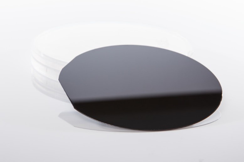
Silicon Wafer Growth
The method used to grow the silicon crystal before it's sliced into wafers influences:
- Material purity
- Oxygen content
- Available resistivity range
- Diameter availability
- Cost and lead time
Silicon wafers are primarily produced using two crystal growth methods— Czochralski (Cz) and Float Zone (Fz).

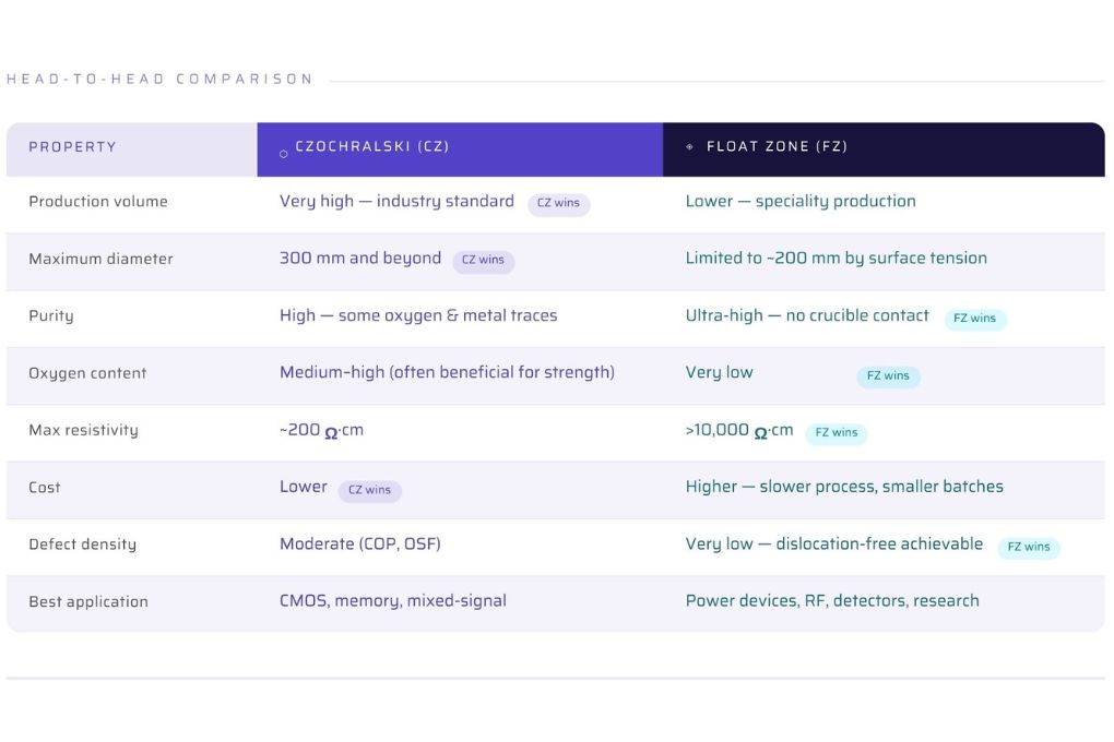
At PI-KEM, we work closely with specialist manufacturers to provide both Cz and Fz materials, with consistent quality, material traceability, and a range of growth options allowing us to support both cost-effective production needs and demanding high-purity applications.
Understanding Silicon Wafer Grades
Not all silicon wafers are created equal. The wafer grade defines its quality, purity, defect density, and surface precision.
Choosing the right grade isn't about always selecting the highest quality – it's about matching quality to purpose.
Key Specifications That Shape Performance
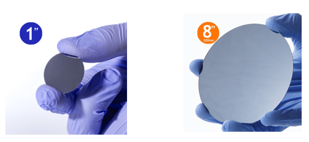
Diameter and Thickness
Wafer size is typically driven by equipment compatibility and handling requirements.
Wafer thickness directly impacts mechanical stability, thermal management and device performance. Thicker wafers are less prone to warping or breakage during high-temperature processing, while thinner wafers enable better heat dissipation, reduced material cost, and improved electrical performance in some devices.
Custom dimensions are available when research demands it, from 1" to 12" (25mm to 300mm) diameters, and custom thicknesses.
Additional tolerance parameters may be specified when flatness is critical:
- Total Thickness Variation (TTV)
- Bow and warp
Crystallographic Orientation
Wafer orientation denotes how the crystal lattices aligns to the wafer surface. It depends on how the wafer was sliced from the silicon ingot. Common orientations, such as <100>, <111>, and <110>, represent different crystal planes with distinct properties.

Orientation influences:
- Mechanical properties
- Electrical behaviour
- Oxidation rates
- Epitaxial growth capacity
- Etching characteristics
Custom orientations are achievable, and features like flats and laser-etching can be incorporated to assist with alignment.
Doping and Resistivity
Doping controls the electrical properties of silicon by introducing charge carriers.
Resistivity is a measure of a materials opposition to the flow of electrical current, and it is a function of dopant concentration. Increasing dopant concentration increases the number of charge carriers, which reduces resistivity. Lower doping levels result in higher resistivity.
Resistivity is measured in Ohm-cm, and typical values are in the 0.001to 10,000 Ohm-cm range.
For many projects, the key starting point is defining:
- N-type, P-type, or undoped
- Required resistivity range
Surface Finish
The wafer surface can be prepared to match processing requirements.
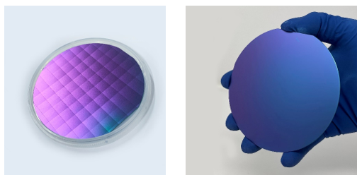
Additional options include:
- Thermal oxide layers
- Metal coatings
- Silicon-on-insulator (SOI)
- Laser marking
Preparing an Enquiry?
If you are ready to request pricing, our Silicon Wafer Technical Guide summarises these parameters into a practical checklist format to help you submit a complete and accurate enquiry.
Download the guide so you can move forward with confidence.
When You Don't Have All the Answers
Here's the reality: you won't always have every specification defined when you first contact us. Requirements may still be evolving, multiple approaches may be under evaluation, or budget and timeline constraints may influence material choices.
Many parameters are interdependent:
- Doping determines resistivity
- Application drives surface finish and grade
- Equipment limits diameter
- Custom specifications affect lead time
This is where working with a knowledgeable partner such as PI-KEM helps translate research goals into practical specifications. A supplier who understands these relationships helps you navigate trade-offs and identify appropriate specifications, mitigating unnecessary cost or complexity.
Flexibility Where it Matters
Silicon wafers are typically supplied in standard boxes of 25, which works well for large-scale research or established production programmes. Early-stage research rarely needs that volume immediately.
As a research-centered supplier, PI-KEM can supply:
- Single wafers or small quantities
- Custom diameters and thicknesses
- Non-standard specifications
This flexibility proves invaluable when you're testing different specifications, validating a new process, comparing growth methods, or simply don't want to commit budget to quantities you won't use this financial year.
Our relationships with specialist manufacturers allow us to support both routine requirements and more demanding or unusual projects. We work closely with you to keep the process clear, efficient, and aligned with both your technical needs and practical constraints.
Working with PI-KEM: Knowledge, Partnership, Results
PI-KEM connects researchers and engineers with high-quality silicon wafers from carefully selected specialist manufacturers.
Our Photonics and Optoelectronics team has over 25 years of experience supporting universities, research institutes, semiconductor companies, and start-ups.
We focus on:
- Understanding your application
- Translating requirements into practical specifications
- Managing lead times and availability
- Helping you avoid unnecessary complexity
Whether you are placing your first order, or managing materials across multiple projects, defining the right specification from the start helps keep your work on schedule and within budget.
Selecting a silicon wafer doesn't need to be a dark art. Start with what you know – your application, process requirements, timeline – and work with a knowledgeable supplier to solidify the technical details.
If you’re ready to request pricing, download our Silicon Wafer Technical Guide for a concise specification checklist.
Not sure which specifications matter for your application? Our specialist team can review your requirements and recommend a practical starting point.
Contact PI-KEM's Photonics and Optoelectronics team today to start the conversation.
📞 Call our technical team on 01827 259250
📧 Email sales@pi-kem.co.uk
📝 Complete our online enquiry form