


Semiconductor Wafer Supply: What's Changing?
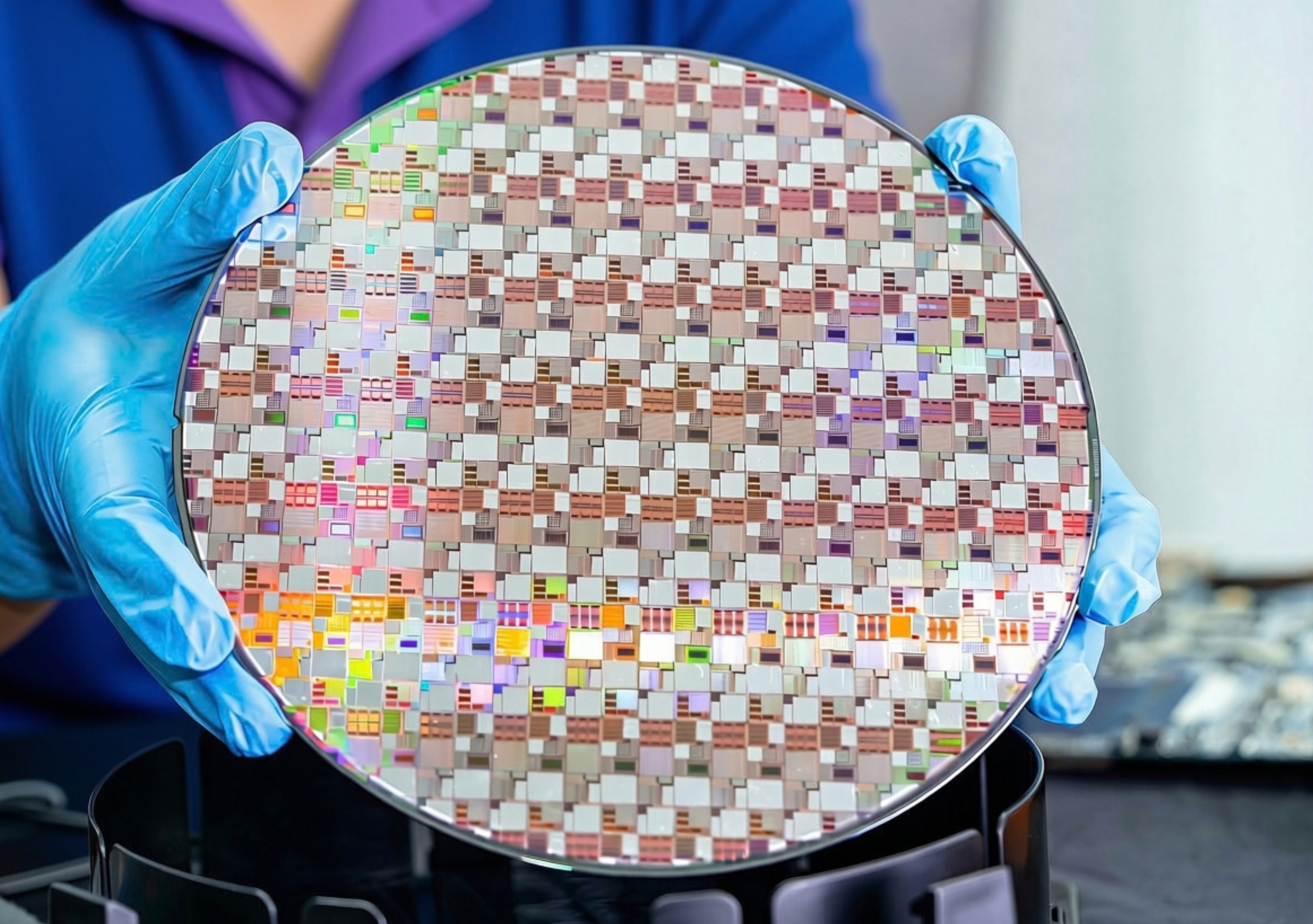
PI-KEM are supporting reliable semiconductor wafer supply.
Changing supply conditions are making planning increasingly important for specialist semiconductor wafer requirements.
For researchers and manufacturers working with compound semiconductors, access to the right wafer is an important part of project planning.
Gallium arsenide (GaAs), indium phosphide (InP), galliumnitride (GaN) and silicon carbide (SiC) wafers support a wide range of applications, including RF and power devices, laser diodes, LEDs, photonics and next-generation sensors.
In recent years, changes to export controls affecting gallium and indium have added complexity to the global supply chain. While SiC is less directly affected by these restrictions, increasing demand across power electronics and other advanced applications is also influencing availability.
For researchers, universities and technology developers, this can mean longer or less predictable lead times and a greater need to plan specialist material requirements in advance.
At PI-KEM, we continue to work closely with specialist supply partners to help customers identify suitable wafer supply routes for their projects.
What is changing in the market?
China accounts for a significant proportion of global gallium and indium refining, and since 2023 additional export licensing requirements have been introduced for both materials.
These changes have added further administration to some international supply routes. At the same time, demand for advanced semiconductor materials continues to grow across applications including electric vehicles, telecommunications, defence, AI, and renewable energy.
Together, these factors mean that sourcing GaAs, InP, GaN and increasingly SiC wafers can require more forward planning than in the past.
What we're hearing from customers
One of the challenges customers are facing is maintaining continuity of supply when an established sourcing route changes or is no longer available.
For example, we recently supported a customer requiring GaAs and InP wafers when their usual supply route was no longer available. Through our trusted supplier network, we were able to identify an alternative source and provide a custom quotation.
Situations like this highlight the value of having access to more than one specialist supply route, particularly where availability or lead times are changing.
How PI-KEM supports specialist wafer requirements
PI-KEM works directly with specialist wafer manufacturers, including D&X, SurfaceNet and MTI Corporation, giving customers access to a broad range of semiconductor wafers, including:
- Gallium Arsenide (GaAs)
- Gallium Phosphide (GaP)
- Indium Phosphide (InP)
- Indium Antimonide (InSb)
- Indium Arsenide (InAs)
- Silicon Carbide (SiC)
- Zinc and cadmium-based II-VI wafers
Our combination of technical understanding and established supplier relationships allows us to investigate different sourcing options, including requirements for specified orientations, dopants, and custom finishing.
We can support projects ranging from early-stage materials research through to device development and more established semiconductor processes.
Planning ahead for specialist wafer requirements
If you're working with GaAs, GaN, InP, SiC or another specialist semiconductor material, speaking to our team early gives us time to investigate the options available for your specification.
Our aim is to make the sourcing process straightforward and help you secure the materials you need for your research or development work.
Talk to our team about your semiconductor wafer requirements
If your usual supply route has changed, lead times have increased or you're looking for a particular wafer specification, our advanced materials team can help.
Share your material, diameter, thickness, orientation, doping, surface finish, quantity, and application requirements, and we'll explore the available options.
Email us: sales@pi-kem.co.uk
Call us: (0) 1827 259250
